- 您现在的位置:买卖IC网 > Sheet目录2004 > LTC1598CG (Linear Technology)IC A/D CONV 12BIT SRL 8CH 24SSOP
10
LTC1594/LTC1598
15948fb
APPLICATIONS INFORMATION
WU
U
OVERVIEW
The LTC1594/LTC1598 are micropower, 12-bit sampling
A/D converters that feature a 4- and 8-channel multi-
plexer respectively. They typically draw only 320
μA of
supply current when sampling at 16.8kHz. Supply cur-
rent drops linearly as the sample rate is reduced (see
Supply Current vs Sample Rate). The ADCs automatically
power down when not performing conversions, drawing
only leakage current. The LTC1594 is available in a 16-pin
narrow SO package and the LTC1598 is packaged in a
24-pin SSOP. Both devices operate on a single supply
from 4.5V to 5.5V.
The LTC1594/LTC1598 contain a 12-bit, switched-
capacitor ADC, sample-and-hold, serial port and an
external reference input pin. In addition, the LTC1594 has
a 4-channel multiplexer and the LTC1598 provides an
8-channel multiplexer (see Block Diagram). They can
measure signals floating on a DC common mode voltage
and can operate with reduced spans to 1.5V. Reducing
the spans allow them to achieve 366
μV resolution.
The LTC1594/LTC1598 provide separate MUX output
and ADC input pins to form an ideal MUXOUT/ADCIN
loop which economizes signal conditioning. The MUX
and ADC of the devices can also be controlled individually
through separate chip selects to enhance flexibility.
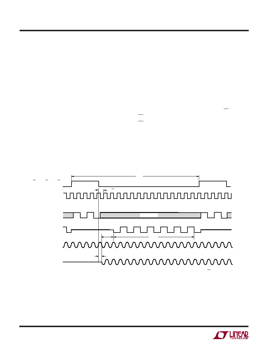
SERIAL INTERFACE
For this discussion we will assume that CSMUX and
CSADC are tied together and will refer to them as simply
CS, unless otherwise specified.
The LTC1594/LTC1598 communicate with the micropro-
cessor and other external circuitry via a synchronous,
half duplex, 4-wire interface (see Operating Sequences in
Figures 1 and 2).
CLK
EN
D1
D2
CSMUX = CSADC = CS
tCYC
B5
B6
B7
B8
B9
B10
B11
Hi-Z
DOUT
CH0 TO
CH7
DIN
tCONV
Hi-Z
tsuCS
NULL
BIT
D0
B4
B3
B2
B1 B0*
tSMPL
tON
DON’T CARE
ADCIN =
MUXOUT
COM = GND
*AFTER COMPLETING THE DATA TRANSFER, IF FURTHER CLOCKS ARE APPLIED WITH CS LOW,
THE ADC WILL OUTPUT LSB-FIRST DATA THEN FOLLOWED WITH ZEROS INDEFINITELY
1594/98 F01
Figure 1. LTC1594/LTC1598 Operating Sequence Example: CH2, GND
发布紧急采购,3分钟左右您将得到回复。
相关PDF资料
LTC1598LCG
IC A/D CONV 12BIT SRL 8CH 24SSOP
LTC1599AIG#TRPBF
IC D/A CONV 16BIT MLTPLYNG24SSOP
LTC1603IG#TRPBF
IC ADC W/SHUTDOWN 16BIT 36-SSOP
LTC1604AIG#TR
IC ADC 16BIT SAMPL SHTDWN 36SSOP
LTC1605-1IN#PBF
IC A/D CONV 16BIT SAMPLNG 28-DIP
LTC1605AISW#TR
IC ADC 16BIT 5V SAMPLING 28SOIC
LTC1606AISW#TRPBF
IC A/D CONV 16BIT SAMPLNG 28SOIC
LTC1608AIG#TRPBF
IC A/D CONV 16BIT SAMPLNG 36SSOP
相关代理商/技术参数
LTC1598CG#PBF
功能描述:IC A/D CONV 12BIT SRL 8CH 24SSOP RoHS:是 类别:集成电路 (IC) >> 数据采集 - 模数转换器 系列:- 标准包装:1 系列:microPOWER™ 位数:8 采样率(每秒):1M 数据接口:串行,SPI? 转换器数目:1 功率耗散(最大):- 电压电源:模拟和数字 工作温度:-40°C ~ 125°C 安装类型:表面贴装 封装/外壳:24-VFQFN 裸露焊盘 供应商设备封装:24-VQFN 裸露焊盘(4x4) 包装:Digi-Reel® 输入数目和类型:8 个单端,单极 产品目录页面:892 (CN2011-ZH PDF) 其它名称:296-25851-6
LTC1598CG#TR
功能描述:IC ADC 12BIT 5V 8CH SAMPL 24SSOP RoHS:否 类别:集成电路 (IC) >> 数据采集 - 模数转换器 系列:- 标准包装:1,000 系列:- 位数:16 采样率(每秒):45k 数据接口:串行 转换器数目:2 功率耗散(最大):315mW 电压电源:模拟和数字 工作温度:0°C ~ 70°C 安装类型:表面贴装 封装/外壳:28-SOIC(0.295",7.50mm 宽) 供应商设备封装:28-SOIC W 包装:带卷 (TR) 输入数目和类型:2 个单端,单极
LTC1598CG#TRPBF
功能描述:IC A/D CONV 12BIT SRL 8CH 24SSOP RoHS:是 类别:集成电路 (IC) >> 数据采集 - 模数转换器 系列:- 标准包装:1,000 系列:- 位数:16 采样率(每秒):45k 数据接口:串行 转换器数目:2 功率耗散(最大):315mW 电压电源:模拟和数字 工作温度:0°C ~ 70°C 安装类型:表面贴装 封装/外壳:28-SOIC(0.295",7.50mm 宽) 供应商设备封装:28-SOIC W 包装:带卷 (TR) 输入数目和类型:2 个单端,单极
LTC1598IG
功能描述:IC A/D CONV 12BIT SRL 8CH 24SSOP RoHS:否 类别:集成电路 (IC) >> 数据采集 - 模数转换器 系列:- 标准包装:1,000 系列:- 位数:16 采样率(每秒):45k 数据接口:串行 转换器数目:2 功率耗散(最大):315mW 电压电源:模拟和数字 工作温度:0°C ~ 70°C 安装类型:表面贴装 封装/外壳:28-SOIC(0.295",7.50mm 宽) 供应商设备封装:28-SOIC W 包装:带卷 (TR) 输入数目和类型:2 个单端,单极
LTC1598IG#PBF
功能描述:IC A/D CONV 12BIT SRL 8CH 24SSOP RoHS:是 类别:集成电路 (IC) >> 数据采集 - 模数转换器 系列:- 标准包装:1,000 系列:- 位数:16 采样率(每秒):45k 数据接口:串行 转换器数目:2 功率耗散(最大):315mW 电压电源:模拟和数字 工作温度:0°C ~ 70°C 安装类型:表面贴装 封装/外壳:28-SOIC(0.295",7.50mm 宽) 供应商设备封装:28-SOIC W 包装:带卷 (TR) 输入数目和类型:2 个单端,单极
LTC1598IG#TR
功能描述:IC ADC 12BIT 5V 8CH SAMPL 24SSOP RoHS:否 类别:集成电路 (IC) >> 数据采集 - 模数转换器 系列:- 标准包装:1,000 系列:- 位数:16 采样率(每秒):45k 数据接口:串行 转换器数目:2 功率耗散(最大):315mW 电压电源:模拟和数字 工作温度:0°C ~ 70°C 安装类型:表面贴装 封装/外壳:28-SOIC(0.295",7.50mm 宽) 供应商设备封装:28-SOIC W 包装:带卷 (TR) 输入数目和类型:2 个单端,单极
LTC1598IG#TRPBF
功能描述:IC A/D CONV 12BIT SRL 8CH 24SSOP RoHS:是 类别:集成电路 (IC) >> 数据采集 - 模数转换器 系列:- 标准包装:1,000 系列:- 位数:16 采样率(每秒):45k 数据接口:串行 转换器数目:2 功率耗散(最大):315mW 电压电源:模拟和数字 工作温度:0°C ~ 70°C 安装类型:表面贴装 封装/外壳:28-SOIC(0.295",7.50mm 宽) 供应商设备封装:28-SOIC W 包装:带卷 (TR) 输入数目和类型:2 个单端,单极
LTC1598LCG
功能描述:IC A/D CONV 12BIT SRL 8CH 24SSOP RoHS:否 类别:集成电路 (IC) >> 数据采集 - 模数转换器 系列:- 标准包装:1,000 系列:- 位数:12 采样率(每秒):300k 数据接口:并联 转换器数目:1 功率耗散(最大):75mW 电压电源:单电源 工作温度:0°C ~ 70°C 安装类型:表面贴装 封装/外壳:24-SOIC(0.295",7.50mm 宽) 供应商设备封装:24-SOIC 包装:带卷 (TR) 输入数目和类型:1 个单端,单极;1 个单端,双极